
Do AVR machines use electron theory? Absolutely! Understanding how AVR microcontrollers function requires delving into the fundamental principles of semiconductor physics and electron behavior. At their core, AVRs are intricate networks of transistors, meticulously arranged to perform complex logical operations. These transistors, built from silicon, rely on the controlled movement of electrons to process information and interact with the external world.
This exploration will unveil the fascinating interplay between electron theory and the inner workings of these ubiquitous devices.
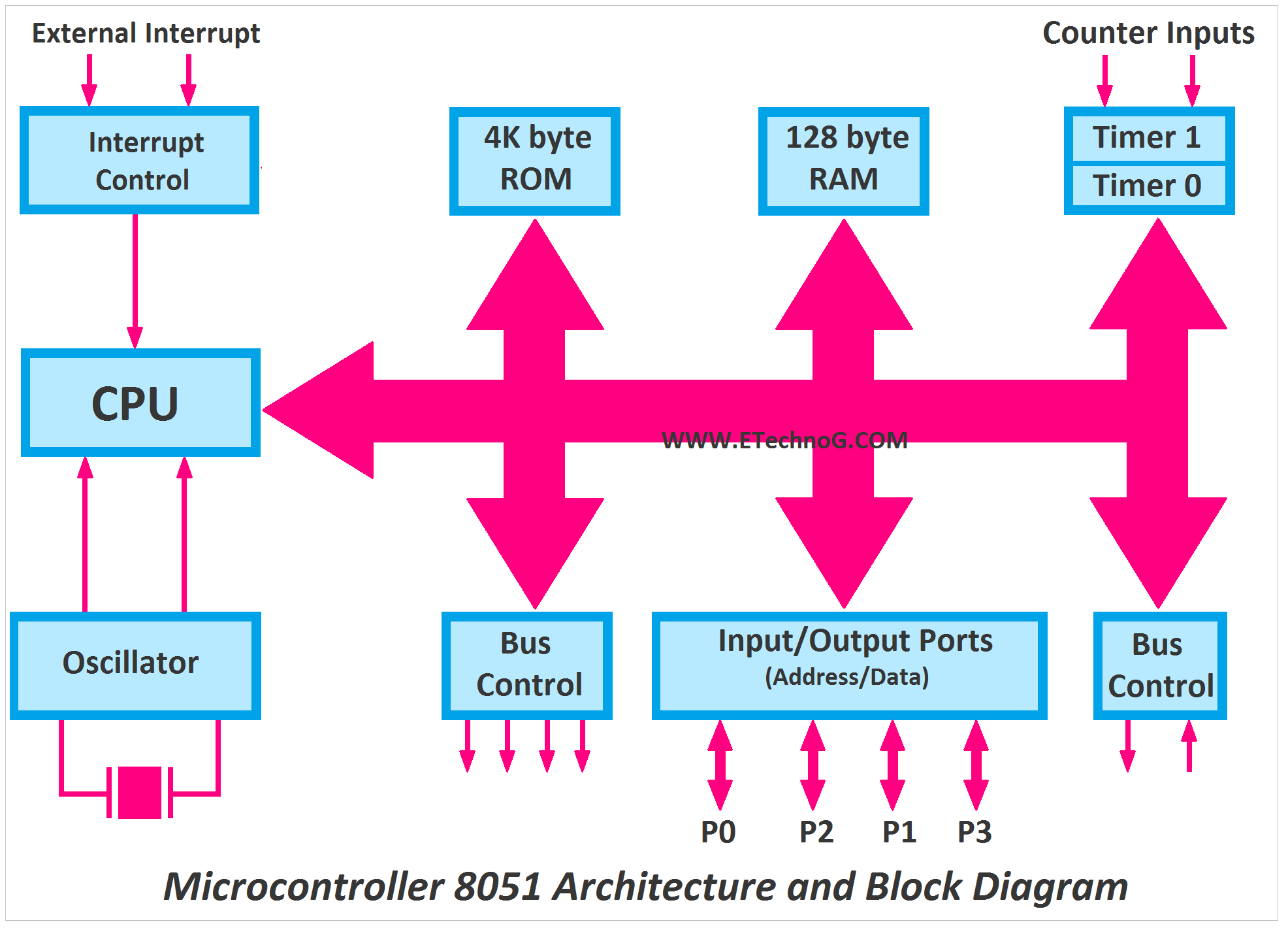
The architecture of an AVR microcontroller, a Harvard architecture with separate program and data memory spaces, is crucial to its operation. The central processing unit (CPU), comprising the arithmetic logic unit (ALU), registers (R0-R31, X, Y, Z pointers, and the Status Register), and other components, orchestrates the execution of instructions fetched from program memory. Data is stored in SRAM and EEPROM, while the clock system synchronizes all operations.
The interplay between these elements, all governed by the precise movement and manipulation of electrons, allows AVRs to perform a vast array of tasks.
Introduction to AVR Microcontrollers
AVR microcontrollers are ubiquitous in embedded systems, powering everything from simple appliances to complex industrial control systems. Their popularity stems from a potent combination of low cost, low power consumption, and a relatively straightforward architecture. This section delves into the heart of these chips, exploring their architecture, core components, and programming.
AVR Microcontroller Architecture: Harvard vs. Von Neumann
AVR microcontrollers employ a Harvard architecture, a significant departure from the more common Von Neumann architecture. In a Von Neumann architecture, both instructions and data share the same memory address space, leading to potential bottlenecks when fetching instructions and data simultaneously. The Harvard architecture, however, utilizes separate memory spaces for program instructions (Flash memory) and data (SRAM and EEPROM).
This allows for simultaneous access to both instructions and data, resulting in significantly faster execution speeds.Imagine a bustling library (Von Neumann): everyone (instructions and data) uses the same catalog and aisles, leading to congestion. Now imagine a specialized research facility (Harvard): separate areas exist for research papers (instructions) and lab equipment/supplies (data), allowing researchers to work more efficiently.A simple diagram would show the CPU at the center, connected to separate buses for program memory (Flash) and data memory (SRAM, EEPROM).
Peripherals are connected to the CPU via various interfaces.
Core Components of AVR Microcontrollers
The AVR CPU is the brain of the operation, comprising several key components:
- Arithmetic Logic Unit (ALU): Performs arithmetic and logical operations on data.
- Registers (R0-R31): 32 eight-bit general-purpose registers provide fast access to data. Think of them as the CPU’s scratchpad.
- Pointer Registers (X, Y, Z): 16-bit registers used for addressing memory locations, acting as highly efficient address pointers.
- Status Register (SREG): Contains flags reflecting the results of arithmetic and logical operations (e.g., carry, zero, negative flags).
Memory is divided into:
- Flash Program Memory: Stores the program instructions; non-volatile, meaning it retains data even when power is off.
- SRAM Data Memory: Stores variables and temporary data; volatile, meaning data is lost when power is off.
- EEPROM: Non-volatile memory for storing configuration data that needs to persist across power cycles; slower access than SRAM.
The clock system provides the timing pulses that synchronize the operation of the microcontroller, while the interrupt system allows the CPU to respond to external events asynchronously.Here’s a table summarizing key registers:
| Register | Description | Size (bits) |
|---|---|---|
| R0-R31 | General Purpose Registers | 8 |
| X | Pointer Register | 16 |
| Y | Pointer Register | 16 |
| Z | Pointer Register | 16 |
| SREG | Status Register | 8 |
AVR Instruction Fetch-Decode-Execute Cycle
The AVR microcontroller executes instructions using the classic fetch-decode-execute cycle. This is a RISC (Reduced Instruction Set Computer) architecture, meaning each instruction typically performs a single operation. The flowchart would depict the cycle:
1. Fetch
The CPU fetches the next instruction from program memory based on the program counter.
2. Decode
The CPU decodes the fetched instruction to determine the operation to be performed and the operands involved.
3. Execute
The CPU executes the instruction, performing the specified operation and updating the relevant registers or memory locations. This may involve different addressing modes (e.g., direct, indirect, register addressing). The program counter is then incremented to point to the next instruction.
Comparison of AVR Microcontroller Families
Different AVR families cater to diverse needs:
| Family | Memory Size | Processing Power | Peripheral Options | Typical Applications |
|---|---|---|---|---|
| TinyAVR | Small | Low | Limited | Simple sensors, remote controls |
| MegaAVR | Medium to Large | Medium to High | Extensive | Motor control, data acquisition |
| XMegaAVR | Large | High | Very Extensive, including advanced peripherals | Complex industrial control, high-speed data processing |
AVR Assembly Language Examples
AVR assembly language provides low-level control over the microcontroller. Here are a few examples:
- Addition:
ADD R16, R17(Adds the contents of R17 to R16) - Subtraction:
SUB R16, R17(Subtracts the contents of R17 from R16) - Bit Manipulation:
SBR R16, 0x01(Sets bit 0 of R16) - Data Movement:
MOV R16, R17(Copies the contents of R17 to R16)
AVR Microcontroller Programming
Programming AVRs typically involves using an ISP (In-System Programming) programmer to upload the compiled code to the microcontroller’s Flash memory. In-circuit debugging tools allow for step-by-step execution and variable inspection during development. Common software tools include AVR Studio and Atmel Studio (now Microchip Studio).
Semiconductor Physics in AVRs

The seemingly magical world of AVR microcontrollers hinges on the surprisingly down-to-earth physics of semiconductors. These tiny chips, the brains behind countless embedded systems, owe their computational prowess to the controlled manipulation of electrons within specially engineered materials. Let’s delve into the fascinating semiconductor physics that makes AVRs tick.
The Role of Semiconductors in AVR Functionality
Semiconductors, primarily silicon in the case of AVRs, form the bedrock of these microcontrollers. Silicon’s unique ability to act as both an insulator and a conductor, depending on the presence of impurities, is exploited to create the intricate network of transistors and logic gates that constitute the AVR’s processing power. This control over conductivity allows for the switching and amplification of electrical signals, the very essence of digital computation.
While other microcontrollers might utilize different semiconductor materials like gallium arsenide (GaAs) – offering advantages in speed for specific applications – silicon’s abundance, cost-effectiveness, and mature manufacturing processes make it the dominant material in the vast majority of AVRs.
| Property | Description | Impact on AVR Performance |
|---|---|---|
| Band Gap Energy | The energy required to excite an electron from the valence band to the conduction band. | A smaller band gap allows for easier electron excitation, leading to faster switching speeds but potentially higher power consumption. A larger band gap results in slower switching but lower power consumption. Silicon’s band gap is carefully chosen for a balance between speed and power efficiency. |
| Electron Mobility | The ease with which electrons move through the material under the influence of an electric field. | Higher electron mobility translates to faster signal propagation and quicker processing speeds within the AVR. Silicon’s mobility, while not the highest among semiconductors, is sufficient for most AVR applications. |
| Resistivity | A measure of a material’s resistance to the flow of electric current. | Lower resistivity allows for efficient current flow, reducing power loss and improving signal integrity. Precise doping controls resistivity in AVRs, optimizing performance and minimizing heat generation. |
P-N Junctions and AVR Operation
The heart of every AVR transistor is the p-n junction, formed by joining p-type (positively doped) and n-type (negatively doped) silicon. This junction acts as a diode, allowing current to flow easily in one direction (forward bias) and blocking it in the other (reverse bias). This rectifying behavior is fundamental to transistor operation. Within an AVR, numerous transistors—both NPN (where current flows from the collector to the emitter when the base is activated) and PNP (where current flows from the emitter to the collector when the base is activated)—are interconnected to create complex logic gates.
A simplified diagram of an NPN transistor would show three terminals (collector, base, emitter) with arrows indicating current flow under forward bias. Similarly, a PNP transistor diagram would show a reversed current flow direction. These transistors, in turn, form the building blocks of the more complex logic gates (AND, OR, NOT, XOR, etc.) that underpin the AVR’s logical operations.
The depletion region, a zone near the junction depleted of free charge carriers, shrinks under forward bias and widens under reverse bias, controlling current flow. A diagram illustrating this would show the depletion region as a gap between the p and n regions, varying in size depending on the applied voltage.
Doping and its Impact on Current Flow
The magic of semiconductor behavior comes from doping – the intentional introduction of impurities into the silicon crystal lattice. Adding elements like boron creates p-type silicon, with “holes” (the absence of electrons) acting as majority carriers. Adding phosphorus creates n-type silicon, with electrons as majority carriers. These majority carriers are responsible for most of the current flow.
Minority carriers (electrons in p-type and holes in n-type) play a crucial role in specific semiconductor phenomena, like the operation of some types of transistors. The doping concentration directly influences the material’s electrical properties, affecting the conductivity, carrier density, and the performance characteristics of the AVR’s transistors and integrated circuits.
The precise control of doping concentration is critical for achieving the desired electrical characteristics in AVR transistors and integrated circuits. Variations in doping can significantly affect the performance, reliability, and power consumption of the device.
Temperature Effects on P-N Junctions in AVRs
Temperature significantly impacts p-n junction behavior. Increasing temperature lowers the forward voltage drop across a p-n junction, meaning less voltage is needed for current to flow. Conversely, reverse saturation current (leakage current) increases with temperature. These temperature-dependent changes can affect the AVR’s operational characteristics, potentially leading to errors or malfunctions. Techniques to mitigate these effects include using temperature-compensating circuits, selecting components with stable characteristics over a wide temperature range, and incorporating thermal management solutions like heat sinks or fans, especially in high-power applications.
For example, an industrial AVR controlling a motor might require a heat sink to prevent overheating and maintain reliable operation in a hot environment.
Electron Flow and Current in AVRs

Electrons, those tiny, negatively charged particles, are the stars of the show in AVR microcontrollers. They’re not just sitting around; they’re zipping and zooming through the intricate circuitry, creating the magic that makes your gadgets tick. Understanding their movement is key to grasping how AVRs function.Think of an AVR chip as a complex network of roads, with electrons acting as the vehicles.
These roads are made of silicon, a material carefully crafted to allow electrons to flow in a controlled manner. The flow of these electrons, driven by the voltage differences applied to the chip, is what we call electric current.
Electron Movement within AVR Circuitry
Electrons don’t actually travel at the speed of light through the AVR. Instead, they move in a more leisurely, “drift” manner. Imagine a crowded stadium where people are trying to move towards an exit. Each individual might only move a small distance, but the overall effect is a significant flow of people. Similarly, electrons bump into atoms within the silicon lattice, causing a gradual overall movement in the direction of the applied electric field.
This drift velocity is surprisingly slow, but the sheer number of electrons involved creates a measurable current.
Current Flow and Electron Movement
Current, measured in amperes (Amps), is the rate at which electric charge flows past a point in a circuit. Since electrons carry a negative charge, conventional current flow is defined as the direction opposite to the actual electron flow. This is a historical quirk; it doesn’t change the underlying physics, just the way we represent it in diagrams.
So, while electrons are drifting one way, the conventional current is depicted as flowing in the opposite direction. It’s like a river; the water flows downstream, but we often describe the river’s flow as going from the source to the mouth, even though the water molecules are moving the other way around.
Types of Current Flow in AVR Circuits
AVRs predominantly utilize direct current (DC), a unidirectional flow of electrons. Think of a battery; it provides a consistent voltage, resulting in a steady current flow in one direction. This is ideal for powering the AVR’s internal components and executing instructions. However, within the AVR’s intricate circuitry, we might see alternating current (AC) signals for specific purposes.
For example, some clock signals used to time the AVR’s operations might be AC signals, oscillating between positive and negative voltages. These are usually at very high frequencies and contained within specific parts of the circuit. The majority of the power and data flow remains DC, ensuring the consistent and reliable operation of the chip.
Voltage and Current Relationships in AVRs: Do Avr Machines Use Electron Theory
AVR microcontrollers, those tiny brains powering everything from washing machines to rockets (well, maybe not rockets
yet*), rely heavily on the dance between voltage and current. Understanding their relationship is key to designing and troubleshooting AVR circuits. Think of it like this
voltage is the pressure pushing electrons, and current is the actual flow of those electrons. Get the balance wrong, and things can get… toasty.
Ohm’s Law, the bedrock of electrical engineering, governs this relationship. It’s surprisingly simple yet incredibly powerful. It states that the current (I) flowing through a conductor is directly proportional to the voltage (V) across it and inversely proportional to its resistance (R). In other words, more voltage means more current, and more resistance means less current. This is beautifully summarized in the equation:
V = I – R
This seemingly simple equation allows us to predict and control the flow of electricity in our AVR circuits. For example, if we know the voltage supplied to a component and its resistance, we can easily calculate the current flowing through it. Conversely, if we know the current and resistance, we can determine the voltage drop across the component. This is crucial for preventing damage to sensitive components and ensuring the proper functioning of the circuit.
Ohm’s Law Application in AVR Circuits
Let’s consider a few practical examples in AVR circuits. Imagine an LED connected to an AVR pin. LEDs have a specific forward voltage (typically around 2V) and a relatively low resistance. If we supply 5V from the AVR, we need to add a resistor in series to limit the current and prevent the LED from burning out. Using Ohm’s Law, we can calculate the appropriate resistor value.
Suppose we want a current of 20mA (0.02A) flowing through the LED. The voltage across the resistor will be 5V (supply voltage)
-2V (LED voltage) = 3V. Therefore, the required resistance is R = V/I = 3V / 0.02A = 150 ohms. Choosing a slightly higher value resistor (e.g., 220 ohms) provides a safety margin.
Voltage and Current in Various AVR Components
Different components in an AVR system exhibit different voltage and current characteristics. For instance, microcontrollers themselves have specific voltage and current requirements. Exceeding these limits can lead to irreversible damage. Similarly, memory chips, sensors, and other peripherals have their own operational voltage and current ranges. Always consult the datasheets for these components to ensure proper operation and avoid damaging them.
A typical AVR microcontroller might operate at 3.3V or 5V, drawing a few milliamps to tens of milliamps depending on its activity level. A sensor, on the other hand, might require a lower voltage and draw a smaller current. Matching the supply voltage and current capacity to the needs of each component is essential for reliable system operation.
Simple Circuit Diagram Illustrating Voltage and Current Interactions
Let’s visualize this with a simple circuit diagram. Imagine a 5V power supply connected to a 220-ohm resistor, which is then connected in series with an LED, and finally connected to ground. The 5V supply provides the voltage. The resistor limits the current flowing through the LED, preventing damage. The LED itself has a voltage drop across it, and the remaining voltage drops across the resistor.
The current is the same throughout the series circuit. This simple circuit beautifully demonstrates Ohm’s law in action, showcasing the voltage drop across different components and the constant current flowing through the series circuit. This fundamental concept forms the basis of more complex AVR circuit designs.
Transistors and Electron Flow in AVRs
AVR microcontrollers, those tiny marvels of modern engineering, wouldn’t be possible without the tireless workhorses of the digital world: transistors. These minuscule switches control the flow of electrons, acting as the fundamental building blocks of all the digital logic that makes your AVR tick. Think of them as incredibly fast and efficient electronic valves, directing the current precisely where it needs to go.Transistors in AVRs act as electronic switches, controlling the flow of electrons based on a small input signal.
This control is what allows AVRs to perform complex calculations and execute instructions. They’re the reason your microcontroller can respond to sensor readings, control motors, and even play a surprisingly catchy tune.
Bipolar Junction Transistors (BJTs) in AVRs
BJTs are three-terminal devices utilizing a current to control a larger current. Imagine a water faucet where a small amount of water pressure (the input current) controls a much larger flow of water (the output current). In a BJT, the current flowing between the collector and emitter terminals is controlled by the current injected into the base terminal.
This current amplification allows for efficient signal amplification and switching within the AVR. BJTs are relatively simple to manufacture, making them cost-effective for high-volume applications. However, they can be slightly less energy-efficient than MOSFETs in some situations.
Metal-Oxide-Semiconductor Field-Effect Transistors (MOSFETs) in AVRs
MOSFETs, unlike BJTs, use an electric field to control the flow of electrons. Think of it as a water gate controlled by a lever; the lever (gate voltage) controls the opening and closing of the gate, allowing or restricting the flow of water (current). A small voltage applied to the gate terminal controls the current flowing between the drain and source terminals.
MOSFETs are generally preferred in modern AVRs due to their higher input impedance (meaning they draw less current from the controlling circuit), lower power consumption, and higher switching speeds. Their prevalence in modern AVRs is a testament to their efficiency and performance.
Transistor Characteristics in AVRs
The choice between BJTs and MOSFETs depends on the specific application and design constraints. The following table summarizes key characteristics:
| Transistor Type | Characteristics |
|---|---|
| BJT | Current-controlled, relatively low input impedance, simple to manufacture, can be less energy-efficient than MOSFETs. |
| MOSFET | Voltage-controlled, high input impedance, lower power consumption, faster switching speeds, more complex to manufacture. |
Transistor Control of Electron Flow in Digital Logic, Do avr machines use electron theory
Transistors are the fundamental building blocks of digital logic gates, such as AND, OR, and NOT gates. By cleverly connecting transistors together, complex logic functions can be implemented. For example, a simple NOT gate uses a single transistor to invert a digital signal: a high input results in a low output, and vice-versa. More complex gates utilize multiple transistors to achieve more intricate logic operations.
Absolutely! AVR machines, at their core, rely on the principles of electron theory to function. Understanding the intricate dance of electrons within semiconductors is key to grasping their operation. For a deeper dive into the foundational physics involved, check out the comprehensive resources available at the skytab knowledge base ; it’s a fantastic starting point for expanding your knowledge.
This foundational understanding will illuminate the sophisticated engineering behind AVR technology and inspire further exploration.
The combination of these gates forms the basis for the intricate circuitry responsible for the AVR’s processing capabilities. These tiny switches, working in concert, enable the complex calculations and decision-making processes within the microcontroller.
Logic Gates and Electron Behavior
The seemingly simple on/off world of digital electronics is actually a bustling metropolis of electrons, zipping and zooming through tiny transistors to create the magic of computation. Understanding how these minuscule particles behave within logic gates is key to grasping the heart of AVR microcontrollers. Let’s delve into the fascinating world where electron flow dictates the outcome of Boolean logic.
Electron Flow in Logic Gates
The fundamental operation of logic gates relies on the controlled movement of electrons within transistors. These transistors, built from semiconductor materials like silicon, act as tiny electronic switches, their conductivity manipulated by the application of voltage. Silicon’s inherent properties, combined with the strategic introduction of impurities (doping), create regions with either an excess of electrons (n-type) or a deficiency of electrons (p-type).
This precise control over electron movement allows for the implementation of logical operations.
In n-type semiconductors, the abundance of free electrons facilitates easy current flow. Imagine a highway teeming with cars (electrons). Conversely, p-type semiconductors have “holes,” or absences of electrons, which act as positively charged carriers. Think of this as a highway with many empty spaces; while cars (electrons) can still move, their flow is less straightforward. The interaction between n-type and p-type regions within a transistor forms the basis for switching behavior.
A NOT gate provides a simple illustration. With no input voltage (logic 0), the transistor is “off,” blocking electron flow. The output remains high (logic 1). Applying an input voltage (logic 1) turns the transistor “on,” allowing electrons to flow, resulting in a low output (logic 0). The diagram would show a single transistor with an input and output, illustrating the electron flow path in both states.
The absence or presence of a continuous flow of electrons through the transistor directly corresponds to the output’s logic state.
Boolean Logic and Electron Movement
The binary nature of digital logic – 0 and 1 – directly maps onto the presence or absence of significant electron flow in a logic gate. A substantial electron flow represents a logic 1, while minimal or no flow represents a logic 0. This seemingly simple mapping is the foundation of complex computations. Transistors, acting as switches, manipulate electron flow to implement Boolean operations.
For example, an AND gate only outputs a logic 1 if both inputs have a logic 1 (substantial electron flow in both input paths). An OR gate outputs a logic 1 if at least one input is a logic 1. The other gates (XOR, NAND, NOR, XNOR) exhibit similar relationships between electron flow and their respective truth tables.
A table summarizing these relationships would show the input logic levels, the corresponding electron flow paths within key transistors, and the resulting output logic level for each gate.
Advanced Logic Gate Analysis
Complex logic circuits are built by cleverly combining basic gates. For instance, a ripple-carry adder uses multiple AND, OR, and NOT gates to perform addition. Tracing the electron flow through such a circuit, given specific inputs, reveals how the individual gate outputs combine to produce the final sum. Propagation delay, the time it takes for a signal to propagate through a gate, arises from the finite electron transit time within the transistors.
This delay is crucial in high-speed circuits.
Different logic gate implementations, like CMOS (Complementary Metal-Oxide-Semiconductor) and TTL (Transistor-Transistor Logic), exhibit varying electron flow characteristics and energy consumption. CMOS, known for its low power consumption, uses both n-type and p-type transistors in a complementary configuration. TTL, an older technology, generally consumes more power. A comparison table would highlight the differences in electron flow patterns and power consumption between these technologies.
Visual Representations
A NAND gate schematic would show two transistors arranged such that their outputs are combined to create an inverted AND operation. Electron flow would be illustrated for various input combinations. Similarly, a NOR gate schematic would show the inverted OR operation using transistors. An XOR gate schematic, depicting the exclusive OR operation, would be more complex, showcasing the interaction of multiple transistors to achieve its unique logic.
A block diagram representing a simple combinational logic circuit would show the interconnected gates, with arrows indicating the flow of signals (and thus electrons) between them.
Simulating electron flow in a logic gate, perhaps using a software like LTSpice or a similar tool, would provide a dynamic visual representation. The simulation would show the changes in electron density and current flow within the transistors as the inputs change, confirming the relationship between electron behavior and logic gate functionality. A detailed description of the simulation’s visualization (without the actual image) would convey the essence of the process.
Memory Operations and Electron Movement
The seemingly simple act of reading or writing data to an AVR microcontroller’s memory involves a fascinating ballet of electrons, orchestrated by the intricate dance of transistors. Understanding this low-level electron movement is key to appreciating the power and limitations of these ubiquitous devices. Let’s delve into the subatomic world within your microcontroller.
Electron Involvement in AVR Memory Read/Write Operations
Memory read and write operations in AVRs rely on manipulating the flow of electrons within transistors to represent binary data (0s and 1s). Changes in voltage and current, driven by these electron movements, dictate the state of memory cells.
Electron Movement During a Memory Read Operation
During a read operation, the address of the desired memory location is presented to the memory controller. This triggers a sequence of events at the transistor level. Consider a simplified SRAM cell (Static Random Access Memory): two cross-coupled inverters (each composed of two transistors, NMOS and PMOS). To read, a select line activates the transistors associated with the targeted memory cell.
If the cell stores a ‘1’, a higher voltage exists across the transistors, resulting in a higher current flow to the output line. Conversely, a ‘0’ would yield a lower voltage and current. The output is then amplified and decoded to produce the digital value.Imagine a simplified circuit: Two NMOS transistors (T1 and T2) and two PMOS transistors (T3 and T4) are arranged in a cross-coupled inverter configuration.
A select line (SEL) controls the access to the memory cell. When SEL is high, T1 and T2 are ON (conducting) and T3 and T4 are OFF (non-conducting) if the stored bit is ‘1’, or vice versa for a stored ‘0’. This allows the stored voltage to be read. A simplified diagram would show the transistors and their connections, with SEL high and the corresponding transistor states for a read operation.
Electron Movement During a Memory Write Operation
Writing a bit to memory involves forcing the appropriate voltage across the transistors of the memory cell. For a ‘1’, a higher voltage is applied, causing a larger electron flow into the storage capacitor (associated with the cell), while a ‘0’ involves a lower voltage, reducing electron flow. SRAM uses transistors to actively hold the charge, while Flash memory uses trapped charge in a floating gate transistor.
EEPROM (Electrically Erasable Programmable Read-Only Memory) utilizes a similar mechanism but with a different transistor structure and a more complex charge trapping and tunneling process. The key difference lies in the mechanism of charge storage and retention. SRAM’s volatile nature means it requires constant power to maintain data; Flash and EEPROM, however, are non-volatile.
Charge Storage in AVR Memory Operations
Different AVR memory types utilize distinct charge storage mechanisms, influencing their performance characteristics.
Comparison of Charge Storage Mechanisms
| Memory Type | Charge Storage Mechanism | Retention Time | Write Speed | Read Speed |
|---|---|---|---|---|
| SRAM | Capacitive charge on transistors; requires constant power to maintain data | As long as power is supplied | Very fast | Very fast |
| Flash | Charge trapped in a floating gate transistor; non-volatile | Many years, potentially decades | Relatively slow (erase/program cycle) | Relatively fast |
| EEPROM | Charge trapped in a floating gate; non-volatile, but with limited write endurance | Many years, potentially decades | Slow (single-byte write) | Relatively fast |
Impact of Leakage Current on Charge Retention
Leakage current, the unwanted flow of electrons through unintended paths, gradually discharges the memory cells. This leads to data loss over time, particularly at elevated temperatures. The rate of charge decay can be modeled using an exponential decay equation:
Q(t) = Q₀
e^(-t/τ)
where:
- Q(t) is the charge at time t
- Q₀ is the initial charge
- τ is the time constant, dependent on leakage current and capacitance.
Higher temperatures increase leakage current, reducing τ and accelerating data loss.
Comparison of AVR Memory Types and Electron-Based Mechanisms
Each memory type employs unique transistor structures and operational principles.
Transistor Structures and Read/Write Operations
SRAM utilizes cross-coupled inverters; Flash uses floating gate transistors; EEPROM employs a similar floating gate but with a different tunneling mechanism. Detailed diagrams showing the transistor-level operation (including cross-sections) of each memory type during read and write cycles would illustrate the differences. These diagrams would depict the relevant transistors, their states (ON/OFF), and the flow of electrons during each operation.
Energy Consumption Differences
SRAM consumes power continuously to maintain data, leading to higher energy consumption compared to Flash and EEPROM, which only consume power during write operations. The differences in energy consumption stem from the different charge storage and retention mechanisms.
Limitations of Each Memory Type
- SRAM: Volatile, limited capacity, higher power consumption.
- Flash: Limited write endurance (number of program/erase cycles), slower write speeds compared to SRAM.
- EEPROM: Very limited write endurance, slower write speeds compared to both SRAM and Flash.
Clock Signals and Electron Synchronization
The heart of any AVR microcontroller beats to the rhythm of its clock signal. This seemingly simple pulse is the driving force behind every instruction, every calculation, and every interaction with the outside world. Understanding how this clock signal is generated, distributed, and utilized is crucial to mastering AVR programming and design. Think of it as the conductor of an incredibly complex orchestra, ensuring every instrument (peripheral) plays in perfect harmony.
The clock signal, a precise sequence of high and low voltage levels, dictates the timing of all operations within the AVR. Its frequency determines the speed at which instructions are executed, directly impacting the microcontroller’s performance and power consumption. Let’s delve into the intricacies of this vital component.
Clock Signal Generation and Distribution within the AVR Microcontroller
The AVR’s clock signal can originate from several sources, offering flexibility in design. The internal RC oscillator provides a readily available, albeit less precise, clock source. For higher accuracy, an external crystal oscillator can be used, offering greater stability and precision. Finally, an external clock source allows synchronization with other systems. The selection and configuration of the clock source are managed through specific registers, primarily the `CLKPR` (Clock Prescaler Register) and `OSC` (Oscillator Control Register) which control the prescaler and oscillator selection, respectively.
Their bit fields dictate the clock source, prescaler division factor, and other clock-related settings. For example, setting specific bits in `CLKPR` allows selection of different prescaler values (e.g., dividing the clock frequency by 1, 8, 64, 256, or 1024), effectively slowing down the clock for lower power consumption or specific peripheral requirements.
Imagine a central clock distribution network within the AVR. The generated clock signal travels from its source (internal RC, external crystal, or external pin) through a series of buffers and dividers. These buffers amplify the signal to ensure sufficient strength for distribution across the various functional units (CPU, peripherals, memory). Dividers reduce the clock frequency to match the requirements of slower peripherals.
This distribution network ensures that all parts of the AVR receive the clock signal with minimal skew, maintaining precise timing across the entire system.
A simplified diagram would show the clock source branching out to various blocks: CPU, SRAM, Flash memory, UART, Timer/Counters, ADC, etc., each potentially having its own clock divider for optimal operation. The lines connecting the source to these blocks would represent the clock distribution network, highlighting the use of buffers to maintain signal strength and integrity.
Clock Signal Control of AVR Operations (Timing Diagrams and Register Details)
The clock signal synchronizes the fundamental fetch-decode-execute cycle of the AVR. Each instruction’s execution is precisely timed by the clock pulses. For instance, a simple ADD instruction might take multiple clock cycles: one for fetching the instruction, one for fetching operands, one for performing the addition, and one for storing the result. A timing diagram would illustrate this, showing the clock signal’s rising and falling edges triggering each step of the instruction execution.
The precise timing depends on the instruction itself and the AVR’s clock frequency.
The clock signal’s role extends beyond the CPU, controlling the operation of peripherals. The UART’s baud rate, for example, is directly linked to the clock frequency and a specific prescaler value configured in registers like `UBRR` (Baud Rate Register). Similarly, Timer/Counters use prescalers (defined in registers like `TCCR0B`) to control their timing resolution, and the ADC’s conversion time is determined by the clock frequency and settings in `ADCSRA` (ADC Control and Status Register A).
| Peripheral | Relevant Registers | Clock Source/Divider | Timing Details |
|---|---|---|---|
| UART | UBRR, UCSRA, UCSRB | System Clock / Prescaler (UBRR) | Baud rate calculation depends on the system clock frequency and the value set in UBRR. Bit timing is precisely controlled by the clock. |
| Timer/Counter0 | TCCR0A, TCCR0B, TCNT0 | System Clock / Prescaler (TCCR0B) | Prescaler settings determine the timer’s counting speed. Overflow interrupts are triggered at precise intervals based on the clock and prescaler. |
| Analog-to-Digital Converter (ADC) | ADCSRA, ADMUX | System Clock / Prescaler (ADCSRA) | Conversion time is directly proportional to the clock frequency and prescaler settings. Sampling rate is also controlled by the clock. |
In essence, the rising or falling edge of the clock signal triggers specific events. For example, a rising edge might initiate data transfer, while a falling edge might signal the completion of an operation. This precise timing is fundamental to the AVR’s deterministic behavior.
Impact of Clock Speed on AVR Performance (Quantitative Analysis)
The relationship between clock speed and execution time is inversely proportional: higher clock speed means faster execution. For example, if a code segment takes 1000 clock cycles at 1 MHz, it will take 500 clock cycles at 2 MHz, resulting in a halving of the execution time. This can be quantified by the simple equation: Execution Time = Number of Clock Cycles / Clock Frequency.
However, increased clock speed comes at the cost of increased power consumption. Power consumption is often related to the clock frequency, though the exact relationship is complex and depends on various factors. A higher clock frequency leads to more switching activity, resulting in higher power dissipation. There’s a trade-off: faster execution versus lower power consumption. Designers often need to balance these competing demands.
Operating at very high clock speeds can lead to challenges. Timing violations might occur if signal propagation delays become significant compared to the clock period. Signal integrity issues can arise due to increased electromagnetic interference. Clock jitter, which refers to variations in the clock’s timing, can introduce inaccuracies and errors into the system’s operation. Higher frequencies necessitate careful consideration of these factors.
Clock Synchronization and External Devices
Synchronizing the AVR’s internal clock with external devices is crucial for many applications. Methods include using external clock sources, phase-locked loops (PLLs), or specialized communication protocols like SPI or I2C with clock synchronization features. Precise timing is essential in real-time control systems, where events must occur at precisely defined intervals. In distributed systems, maintaining synchronization among multiple AVRs presents significant challenges, requiring careful consideration of clock drift, latency, and communication protocols.
These challenges often involve sophisticated techniques to maintain a consistent and accurate time base across all nodes.
Power Consumption and Electron Flow

Power consumption in AVR microcontrollers is intrinsically linked to the movement of electrons. Think of it like this: every calculation, every instruction executed, every blink of an LED – it all boils down to electrons flowing through tiny pathways within the chip. The more electrons are jostled around, the more power is consumed. Understanding this relationship is key to designing energy-efficient AVR applications.Electrons, those tiny negatively charged particles, are the heart of the matter.
Their flow constitutes an electric current, and the rate of this flow, combined with the voltage across the circuit, determines the power consumed (P = IV, where P is power, I is current, and V is voltage). In AVRs, various components, such as the CPU, memory, and peripherals, all draw current, and the sum of these currents determines the overall power consumption.
A higher current means more electrons are moving, leading to higher power usage.
Power Consumption Reduction Techniques
Reducing power consumption in AVR applications involves cleverly managing electron flow. This can be achieved through a variety of strategies, each aiming to minimize the number of electrons in motion when not absolutely necessary.
One key technique is careful selection of clock frequency. A faster clock means more instructions are executed per second, but also means more electron movement and higher power consumption. Lowering the clock frequency when possible (e.g., during idle periods) can dramatically reduce power usage. Imagine a highway: a slower speed limit means fewer cars (electrons) are moving at any given time.
Another important aspect is power-saving sleep modes. AVRs offer various sleep modes that significantly reduce power consumption by putting parts of the chip to sleep. In deep sleep, for instance, only a minimal amount of circuitry remains active, drastically reducing electron flow and thus power consumption. This is like putting your car in park – the engine is off, and fuel consumption (electron flow) is virtually zero.
Power Optimization Examples
Let’s consider a real-world example: a wireless sensor node powered by a small battery. The node periodically collects sensor data and transmits it wirelessly. To maximize battery life, we can employ several power-saving techniques. First, we could use a low-power radio transceiver, which minimizes current draw during transmission. Second, we could put the AVR into a low-power sleep mode between data collection cycles.
Finally, we can use a low clock frequency during data processing to minimize the overall electron flow and reduce power consumption. This careful balancing of electron movement extends battery life significantly. Consider another example: a battery-powered alarm clock. During operation, the clock requires a certain level of current to display time and other functions. But during the night, we can program it to reduce the frequency of its internal clock, resulting in less electron flow and, thus, lower power consumption, extending the battery’s lifespan.
Interrupts and Electron Flow Changes
Imagine the AVR microcontroller as a tiny, incredibly busy conductor orchestrating a symphony of electrons. Normally, it follows a meticulously planned score, executing instructions one after another. But sometimes, a particularly insistent musician (an external event) demands the conductor’s immediate attention. This is where interrupts come in, causing a dramatic shift in the electron flow, a sudden change of tempo in our electronic symphony.Interrupts momentarily divert the electron flow from the main program execution to handle a higher-priority task.
This is achieved by altering the microcontroller’s internal state, specifically the program counter (which dictates the next instruction to be executed) and the context of the currently running program (saving its state so it can resume later). The electrons, instead of following the pre-determined path, are momentarily rerouted to a specific interrupt service routine (ISR). Think of it as a sudden detour on a highway, where the main traffic flow is temporarily redirected to deal with an emergency.
Interrupt Handling Steps
The process of handling an interrupt involves a precise sequence of events, all driven by the underlying electron flow changes within the AVR. The entire process is incredibly fast, happening in microseconds, but the steps are distinct.First, the interrupt request (IRQ) signal arrives. This signal, an electrical pulse, indicates that an external event has occurred, requiring immediate attention. This signal triggers a change in the electron flow, essentially a switch that redirects the current to the interrupt circuitry.
The microcontroller then identifies the source of the interrupt, a process involving checking different interrupt vectors. Each vector is like a specific address in the microcontroller’s memory that points to the corresponding ISR.Next, the current state of the main program (the registers holding data and the instruction pointer) is saved onto the stack. This is crucial to resume the main program after the interrupt is handled.
This saving process involves moving electrons into specific memory locations, changing their flow pattern to perform a series of memory write operations. The program counter is then updated to point to the start address of the ISR.The ISR is then executed. This is where the specific task related to the interrupt is handled. This execution involves manipulating electrons within the AVR’s logic gates and memory, changing the flow to perform calculations, data transfers, and other operations specific to the interrupt’s function.
Think of this as the conductor focusing their attention on the soloist who needs immediate attention.Finally, after the ISR completes, the saved state of the main program is restored from the stack. This involves reading data from memory locations, again redirecting electron flow to specific memory locations. The program counter is restored to its original value, resuming execution of the main program exactly where it left off.
The electron flow seamlessly returns to its original path, continuing the main program’s execution. The entire process is remarkably efficient and precise, showcasing the elegant control the AVR has over electron flow.
Peripheral Interactions and Electron Flow
The seemingly simple act of an AVR microcontroller communicating with a peripheral device is, at its core, a complex ballet of electrons. Understanding this electron flow is crucial for designing efficient and reliable embedded systems. This section delves into the fascinating world of peripheral interaction from an electron’s-eye view, exploring the mechanisms, protocols, and potential pitfalls along the way.
Peripheral Interaction at the Hardware Level
Understanding how peripherals connect to an AVR requires a look at the physical layer. This involves examining the electrical signals and their pathways.
Detailed Schematic: Imagine a simplified schematic of an ATmega328P microcontroller interacting with a UART (Universal Asynchronous Receiver/Transmitter). The ATmega328P’s PD0 pin (RXD) is connected to the UART’s RX pin, receiving data. The PD1 pin (TXD) connects to the UART’s TX pin, sending data. Both microcontroller and UART share a common ground (GND) and are powered by a 5V supply (VCC).
A crystal oscillator provides the clock signal for the microcontroller. The UART’s TX and RX lines represent the data flow, with GND providing the reference point for voltage levels. VCC provides the power for both the microcontroller and the UART. The crystal oscillator provides the timing reference for the microcontroller’s internal operations, indirectly influencing the timing of data transmission.
Absolutely! AVR machines, at their core, rely on the principles of electron theory to function. Understanding the intricate dance of electrons within semiconductors is crucial to grasping their operation. For a deeper dive into the underlying physics and related technological concepts, consult the comprehensive resources available at the llm knowledge base. This invaluable resource will illuminate the fascinating connection between electron behavior and the sophisticated engineering behind AVR technology, empowering you to explore this field further.
The power of understanding electron theory unlocks a world of possibilities in AVR machine design.
Electron Flow Visualization: Picture a simplified representation. During a bit transmission, electrons flow from the 5V VCC supply towards the TXD pin when a ‘1’ is sent; a high voltage is present, and a substantial current flows. When a ‘0’ is sent, the TXD pin is pulled low (near 0V), and the electron flow is significantly reduced. The RXD pin operates similarly, but in reverse: electrons flow towards the microcontroller when a high voltage is received, indicating a ‘1’.
Different colored lines (e.g., blue for TXD, red for RXD) could visually represent the direction and voltage level of the signals.
Timing Diagram: Visualize a timing diagram showing the transmission of a byte. The horizontal axis represents time, and the vertical axis represents the voltage levels of TXD, RXD, and the clock signal. The clock signal is a square wave, and data bits are transmitted at specific intervals synchronized to the clock. Each bit is represented by a high or low voltage level on the TXD line, and these levels are sampled by the RXD line at the receiving end.
Timing events include the start bit, data bits, parity bit (if used), stop bit, and any acknowledge signals.
Data Transfer Mechanisms and Electron Flow
Different communication protocols utilize distinct methods to manage the electron flow for data transmission.
Specific Protocol Analysis (UART): In UART, transmitting a character involves sending a start bit (low voltage), followed by data bits (high or low voltage representing 1s and 0s), a parity bit (optional), and a stop bit (high voltage). Electrons flow from the VCC to the TXD pin during high voltage levels and minimally during low voltage levels. The RXD pin mirrors this, with electrons flowing towards the microcontroller during high voltage levels on the received signal.
Specific Protocol Analysis (SPI): SPI uses MOSI (Master Out Slave In), MISO (Master In Slave Out), SCK (Serial Clock), and SS (Slave Select) lines. The master controls the SCK, clocking data out on MOSI and receiving data on MISO. Electrons flow on MOSI and MISO according to the clock pulses and the data being transmitted or received. The SS line controls which slave device is active, affecting the electron flow on MOSI and MISO accordingly.
Specific Protocol Analysis (I2C): I2C uses SDA (Serial Data) and SCL (Serial Clock) lines. Data is transmitted as voltage levels on SDA, synchronized by SCL. Start and stop conditions are defined by voltage transitions on SDA. Acknowledge bits are sent by the slave device, influencing the electron flow on SDA. Multi-master arbitration involves contention on SDA and SCL lines, with a priority mechanism deciding which master gains control of the bus, influencing the timing and flow of electrons.
Electron Flow and Communication Protocol Efficiency
The efficiency of data transfer is heavily influenced by the protocol’s handling of electron flow.
Comparison Table: A comparison table could show that SPI generally offers higher data transfer rates than UART and I2C due to its parallel nature (multiple data bits transmitted simultaneously). I2C, while slower, typically consumes less power than SPI or UART due to its simpler hardware requirements and lower clock speeds. UART falls somewhere in between in terms of both speed and power consumption.
Noise Immunity Analysis: Signal strength, impedance matching, and the use of differential signaling all impact noise immunity. Protocols with higher signal strength and better impedance matching tend to have better noise immunity. Differential signaling, often employed in high-speed applications, improves noise immunity significantly.
Power Consumption Analysis: A bar chart could visually compare the power consumption of UART, SPI, and I2C under different conditions. Factors like clock speed and data rate heavily influence power consumption. Higher clock speeds and higher data rates generally lead to increased power consumption across all three protocols.
Analog-to-Digital Conversion (ADC) and Electron Behavior
The seemingly simple act of converting an analog signal – a smoothly varying voltage representing, say, the temperature of a room – into a digital signal, a series of discrete numbers, is a surprisingly complex dance of electrons. Inside an AVR microcontroller, this conversion, performed by the ADC, relies on a delicate manipulation of electron flow, a process we’ll explore here.
Think of it as a tiny, high-speed translator, whispering the secrets of the analog world to the digital realm.The ADC conversion process involves two key stages: sampling and quantization. Sampling is like taking snapshots of the analog signal at regular intervals; quantization is then assigning a discrete numerical value to each snapshot. The interplay of electrons in these stages is fascinating and crucial for accurate conversion.
Sampling in the ADC
Sampling involves measuring the analog input voltage at specific time intervals. This measurement is fundamentally about determining the density of electrons at the input pin. A higher voltage means a higher electron density, a lower voltage a lower density. The sampling circuit effectively counts these electrons (or rather, measures the resulting charge), providing a snapshot of the analog signal’s amplitude at that instant.
The speed and accuracy of this electron “counting” directly affect the fidelity of the digital representation. Imagine it as a tiny, incredibly fast photographer capturing the fluctuating electron density. The faster the shutter speed (sampling rate), the more accurately the change in the signal is represented.
Quantization in the ADC
Once the analog voltage is sampled, the quantization stage comes into play. This stage converts the continuous range of voltage values into a finite set of discrete digital values. Think of it as dividing the voltage range into a number of equally sized “bins.” Each bin is assigned a unique digital code. The electron density measured during sampling determines which bin the sampled voltage falls into, and the corresponding digital code is assigned.
The number of bits used to represent each digital value determines the resolution of the ADC. More bits mean more bins, and therefore a more precise representation of the analog signal. A higher resolution means a more accurate picture of the electron density, but it also requires more memory and processing power.
Noise and Electron Flow in ADC Processes
The enemy of accurate ADC conversion is noise. Noise manifests as unwanted fluctuations in the electron flow, either originating from the analog signal itself or introduced during the conversion process. This noise can cause errors in the sampling and quantization stages, leading to inaccurate digital representations. Imagine the photographer’s camera shaking slightly, blurring the picture of the electron density.
Various techniques, such as filtering and averaging, are used to mitigate the effects of noise and improve the accuracy of the ADC. For example, averaging multiple samples helps to reduce the impact of random noise fluctuations. The more samples averaged, the better the noise suppression. This is similar to taking multiple photos and averaging their pixel values to reduce noise in an image.
Different types of noise, such as thermal noise and shot noise, influence electron flow differently, requiring different mitigation strategies.
Illustrative Example: A Simple AVR Circuit

This section details a straightforward AVR circuit showcasing fundamental microcontroller operations, specifically input/output (I/O) control and timing. We’ll illuminate an LED based on the state of a push button switch, a classic demonstration of embedded systems principles. The electron flow within the circuit will be explained in detail, emphasizing the interplay between the microcontroller’s internal workings and the external components.
Circuit Schematic
Imagine a schematic diagram, drawn using a tool like Fritzing. The diagram would feature an ATmega328P microcontroller at its heart. Pin 13 of the microcontroller connects to the positive leg of a 220Ω resistor, which in turn connects to the positive leg of a red LED. The negative leg of the LED is connected to ground. A push-button switch is connected between pin 2 of the microcontroller and ground.
A 10kΩ resistor connects pin 2 to the microcontroller’s VCC (5V). All connections are clearly labeled with pin numbers and voltage levels. The legend would define the symbols used for the microcontroller, LED, resistor, and switch. This configuration utilizes a pull-up resistor to ensure a defined high state when the button is not pressed.
Circuit Operation
When the button is not pressed, the 10kΩ pull-up resistor holds pin 2 high (5V). The microcontroller’s internal circuitry, specifically the I/O port, registers this high state. The microcontroller’s program, running on its CPU, checks this pin’s state regularly (either through polling or an interrupt). When the button is pressed, the circuit to ground is completed, pulling pin 2 low (0V).
This change in voltage triggers an event (either an interrupt or a change in the polled value) within the microcontroller. The microcontroller’s program responds by changing the state of its output pin (pin 13), which toggles the LED’s on/off state. This involves internal transistor switching within the microcontroller’s I/O circuitry, altering the current flow to the LED. The 220Ω resistor limits the current to prevent damage to the LED.
Circuit Component Details
AVR Microcontroller (e.g., ATmega328P): This acts as the central processing unit, reading the button’s state and controlling the LED. Internal transistors switch on and off, altering current flow to the LED based on the program’s instructions. Specific registers like PORTB (for I/O) and DDRB (for direction control) are used to manage the I/O pins. Electrons flow within the microcontroller’s silicon structure, guided by the transistor gates’ states, determined by the program’s logic.LED (Light Emitting Diode): The LED illuminates when electrons flow through it from its negative (cathode) to its positive (anode) leg. This flow of electrons causes recombination with holes in the semiconductor material, releasing energy as photons (light). A typical red LED requires approximately 2V forward voltage and 20mA current.Push Button Switch: This simple switch acts as a current interrupter. When pressed, it creates a closed circuit between pin 2 and ground, allowing electrons to flow and pulling the pin low. When released, the circuit is open, and the pull-up resistor holds the pin high.Resistors (220Ω and 10kΩ): The 220Ω resistor limits the current flowing through the LED, preventing damage. Ohm’s Law (V=IR) dictates the voltage drop across it. The 10kΩ resistor acts as a pull-up resistor, ensuring a defined high state on pin 2 when the button is not pressed, providing a stable input for the microcontroller.
AVR C Code
“`c//Simple LED toggle with button press#include Programming typically involves using the Arduino IDE or a similar AVR programming environment. The compiled C code is uploaded to the microcontroller via an AVR programmer (e.g., an Arduino Uno acting as an ISP, or a dedicated programmer like USBasp). The process involves selecting the correct board type (ATmega328P) in the IDE, compiling the code, and then using the programmer to upload the compiled hex file to the microcontroller’s flash memory. This process writes the instructions to the microcontroller, enabling it to execute the program and control the LED based on the button presses. What is the difference between a RISC and a CISC architecture, and which does the AVR use? RISC (Reduced Instruction Set Computer) architectures, like the AVR, utilize simpler instructions executed quickly, while CISC (Complex Instruction Set Computer) architectures use more complex instructions that take longer to execute. The AVR uses a RISC architecture. How does temperature affect the lifespan of an AVR microcontroller? High temperatures accelerate the degradation of semiconductor materials, potentially leading to reduced lifespan and increased failure rates. Operating AVRs within their specified temperature range is crucial for reliability. What are some common troubleshooting techniques for AVR programming? Common troubleshooting involves checking power supply, verifying connections, using a logic analyzer to inspect signals, and systematically debugging code using an in-circuit debugger. Can AVRs handle real-time applications? Yes, AVRs with their interrupt system and precise timing capabilities are suitable for many real-time applications, though the complexity of the application and required response times will dictate the choice of specific AVR and clock speed.Circuit Component Summary
Component Specification Function AVR Microcontroller ATmega328P Controls the LED based on button press. LED 5mm Red, 20mA, 2V Indicates button press state. Push Button Switch SPST, Normally Open Provides input to the microcontroller. Resistor (LED) 220Ω Limits current to the LED. Resistor (Button) 10kΩ Pull-up resistor for the button switch, ensuring a defined high state when not pressed. Programming the AVR Microcontroller
FAQ Overview

